
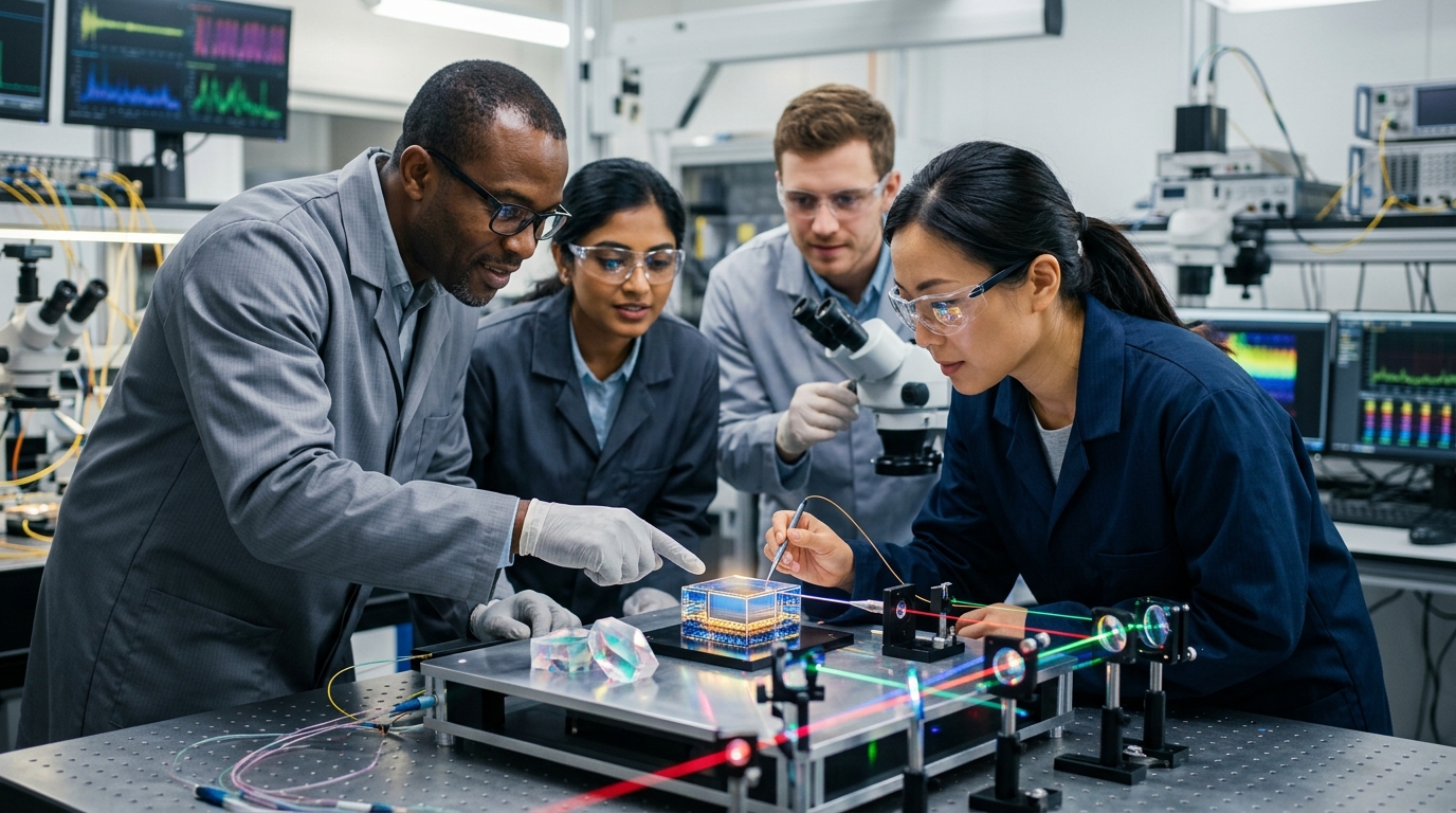
For 70 years, every significant computer has been built on silicon. However, in the last 18 months, American laboratories have developed revolutionary alternatives to address silicon’s physical limitations. Bringing over 15 years of experience in the digital information field to the forefront, Pariganaka.com recognizes this shift away from traditional semiconductors as a critical turning point for global technology.
The Physical Limits of Traditional Chips
Silicon is hitting a physical wall due to heat generation and quantum tunneling. As transistors shrink to atomic scales, electrons leak through barriers, wasting power and generating excess heat. Furthermore, AI data centers training massive models on traditional chips consume enormous amounts of electricity, with a large portion of that energy simply wasted on industrial cooling systems. To solve this, engineers are pioneering completely new computing materials and architectures.
Photonic Computing: Thinking with Light
Instead of relying on electricity, new processors use light for computation.
- A Boston-based company has demonstrated an AI processor that runs models using beams of light.
- Light naturally performs the complex matrix multiplications required for artificial intelligence as it passes through microscopic waveguides.
- This method drastically reduces energy consumption and heat generation while maintaining accuracy comparable to traditional electronic chips.
- Because light does not fight resistance like electrons, dozens of parallel computations can travel down the same optical channel simultaneously without interfering with one another.
Neuromorphic Architecture: Brain-Inspired Systems
Engineers have created brain-inspired computers to bypass the traditional computing bottleneck known as the “memory wall”.
- A system named “Hollow Point” at Sandia National Laboratories features over a billion artificial neurons.
- Unlike standard chips that constantly draw power by operating on a continuous clock, neuromorphic chips remain silent and consume almost zero energy until they receive a signal to process.
- These chips process and store memory in the exact same location. This eliminates the massive energy costs associated with constantly shuttling data back and forth across the processor.
- On certain tasks, this architecture delivered answers dozens of times faster than conventional processors while using up to a hundred times less energy.
Cubic Boron Arsenide: The Ultimate Material
This newly refined crystal is being hailed by researchers as potentially the best semiconductor ever discovered.
- Despite containing heavy arsenic atoms, it moves heat almost ten times better than silicon, directly solving the thermal bottleneck of modern computing.
- It also conducts electrical charge—both negative electrons and positive “holes”—significantly faster than silicon.
- By pulling heat away exceptionally fast and handling higher voltages without leaking current, this material could eventually render silicon entirely unnecessary.
Atom-Thin Skyscraper Chips
Researchers have successfully grown single sheets of a semiconductor called molybdenum disulfide, which are exactly three atoms thick.
- These ultra-thin layers physically prevent quantum tunneling because electrons simply have no extra space to wander into.
- Using a dual-zone furnace, engineers can grow these atomic sheets at low temperatures directly on top of older silicon chips without causing heat damage to the base layer.
- This technique allows for the creation of 3D “skyscraper” chips where memory and processing logic are stacked vertically. Data only has to travel a few atoms upward instead of millimeters across a flat 2D surface.
The technology industry is no longer constrained by the natural limitations of the materials we pull from the earth. By designing custom materials and architectures from the atomic level upward, the next era of computing will prioritize extreme efficiency, unprecedented speed, and new architectural paradigms.
Leave a Reply